Hemeixin Electronics Co.,Ltd.
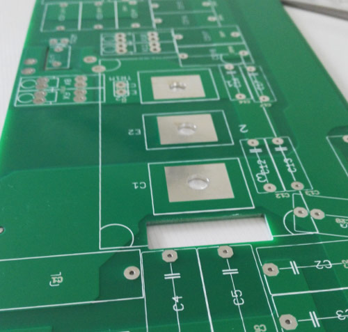
Hemeixin Electronics Ltd is one quick-turn manufacturing platform of prototype, various types and low volume PCBs in the world; to offer personalized one-stop solution matching the local various types and quick SMT service
We specialize in Quick turn PCB services with an industry leading turnaround time as fast as 72 hours.
Not only do we know the importance of ensuring quick turnaround for the success of your project, but we also know that the resulting quality is equally as important. With our integrated in-house facility, 687-strong workforce, 87-plus dedicated engineer, 42 different PCB processing stations, and 24/5 production schedule, we can fulfill all PCB prototype projects on tight deadlines faster than the average lead times most PCB service companies can achieve - and with quality, of course. This means the shortest turnaround times and the highest quality for any HDI project as well.
When your company needs fast and rapid PCB prototyping, know that you can count on Hemeixin to deliver high quality printed circuit boards on time at competitive prices.
We have an industry leading on-time percentage that customers have come to love. We understand the importance of delivering on our promises, so we have a rock solid customer satisfaction guarantee.
Welcome to our website! We like you to receive your order ASAP and with the least possible cost. To get your order requirements easily to us, take any of the following steps:
1. You can use our online calculate from website: www.hemeixinpcb.com .
2. Email sales@hemeixinpcb.com for any question or support you need and get a reply within 24 hours.
3. Call: +86 0755-2758-6529, or Skype: Hemeixin.He talk to us directly for any questions or concern regarding your board project.
4. You can easily send requests and inquiries at http://pcbonline.hemeixinpcb.com/.